


A Novel SiC Trench MOSFET Structure with Enhanced Short Circuit Robustness
ID:15
Submission ID:127 View Protection:PUBLIC
Updated Time:2021-07-21 20:00:47 Hits:1082
Poster Presentation
Start Time:2021-08-27 12:52 (Asia/Shanghai)
Duration:1min
Session:[P] Poster » [P1] Poster 1
Abstract
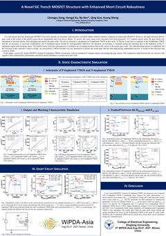
It is well known that SiC trench-gate MOSFET has advantage in conduction performance with narrower cell pitch, higher channel mobility and lower specific on-resistance (Rdson,sp) compared to planar-gate MOSFET. However, the high electrical field in gate oxide at the corner of the trench is the major concern for the trench-gate MOSFET, which may cause device degradation and/or device failure[1]. To resolve this issue, J. Tan introduced a P+ implant region under the gate trench to provide electric field shielding and protect the gate oxide[2] as shown in Fig.1(a). The device structure is designated as P-implanted TMOS in this work. The P+ implant region would make the effective N-epi layer for blocking voltage thinner, thus making device breakdown voltage lower. And, additional connection path between the P+ implant and the source electrode should be provided to recover charge during the switch-on transient. In this paper, a novel SiC trench MOSFET (named N-implanted TMOS) with N-implant region introduced under the gate trench is proposed, as shown in Fig.1(b). The comparsion study between the two devices with regard to static characteristic performance and short circuit robustness are carried out in this work. The key structural parameters of the two devices are listed in Table 1.
Keywords
SiC trench MOSFET,short circuit capability
Speaker

Comment submit