An Optimal Design Scheme of Intermediate Bus Voltage for two-stage LLC Resonant Converter Based on SiC MOSFET
ID:6
Submission ID:145 View Protection:PUBLIC
Updated Time:2021-08-05 19:10:34
Hits:1202
Poster Presentation

Start Time:2021-08-27 13:01 (Asia/Shanghai)
Duration:1min
Session:[P] Poster » [P1] Poster 1
Abstract
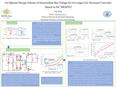
The two-stage LLC resonant converter has numerous superiority than conventional LLC resonant converter in wide voltage input and low voltage high current output occasions. The non-isolated converter functions as a pre-regulator to regulate the output voltage, whereas the LLC resonant converter can operate at a fixed switching frequency slightly lower than the resonant frequency, thereby a high efficiency could be achieved. Besides, the fixed-frequency operating state of LLC is conducive to the optimal design of magnetic components. In such a two-stage converter system, the optimal design of the intermediate bus voltage is of great significance. This parameter not only determines the voltage of switches, but also affects the efficiency of the entire converter. To optimize the overall performance of the converter, a majorized design scheme of intermediate bus voltage is proposed. This method target to the compromise between efficiency and the voltage of tubes. The optimal point is obtained via building and solving the mathematical model. Simulations is conducted to verify the effectiveness of the proposed design methodology.
Keywords
two-stage LLC resonant converter, high power density, optimal design
Speaker


Comment submit