


DC Transform Circuit Design Based on Multiplier Rectification
ID:8
Submission ID:139 View Protection:PUBLIC
Updated Time:2021-08-05 19:13:43
Hits:1091
Poster Presentation
Start Time:2021-08-27 12:59 (Asia/Shanghai)
Duration:1min
Session:[P] Poster » [P1] Poster 1
Abstract
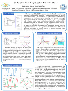
Due to the high reliability and high efficiency, the DC/DC converters are rapidly developing. However, a challenge is faced which is the output voltage range of the DC/DC converter is limited by the withstand voltage of the device in practice. In order to solve this problem, this paper designs a DC/DC conversion circuit based on the voltage double rectifier circuit and half-bridge LLC topology. It realizes high voltage output under the condition of low voltage input. Meanwhile, the requirements for the withstand voltage of the device are relaxed, which is convenient for the selection of the device. Furthermore, the zero voltage switch (ZVS) of the primary-side switches and the zero current switch (ZCS) of the secondary-side diodes can be achieved. The correctness and effectiveness of the proposed method are finally verified by simulation.
Keywords
Multiplier Rectification, zero current switching, the withstand voltage of the device, DC/DC converter, LLC resonant circuit
Speaker

Comment submit