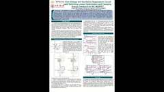
Over-Voltage and Oscillation Suppression Circuit with Switching Losses Optimization and Clamping Energy Feedback for SiC MOSFET
ID:64
Submission ID:15 View Protection:PUBLIC
Updated Time:2021-07-21 20:02:30 Hits:1361
Poster Presentation

Start Time:2021-08-27 12:04 (Asia/Shanghai)
Duration:1min
Session:[P] Poster » [P1] Poster 1
Abstract
The snubber circuit is a cost-effective solution to reduce the serious turn-off over-voltage and oscillation caused by the fast switching characteristics of SiC MOSFET. However, the turn-on switching losses will significantly increase due to the snubber decouples the power loop parasitic inductance during the switching process. In this paper, a SiC MOSFET over-voltage and oscillation suppression circuit (OVSC) with not only switching losses optimization feature but also the clamping energy feedback characteristic is proposed. The over-voltage and oscillation can be effectively suppressed by clamping capacitors, and those capacitors do not participate in the switching process until the over-voltage occurs, which is of benefit to the switching losses reduction compared with RC snubber circuits. Besides, the turn-off over-voltage and oscillation energy stored in clamping capacitors can be feedback to DC and load side through a passive branch composed of an energy feedback inductor and a diode. Experimental results show that OVSC has excellent over-voltage and oscillation suppression performance, and can significantly reduce switching losses compared with RC snubber circuits.
Keywords
SiC MOSFET, over-voltage and oscillation, snubber circuit, switching losses optimization.
Speaker


Comment submit